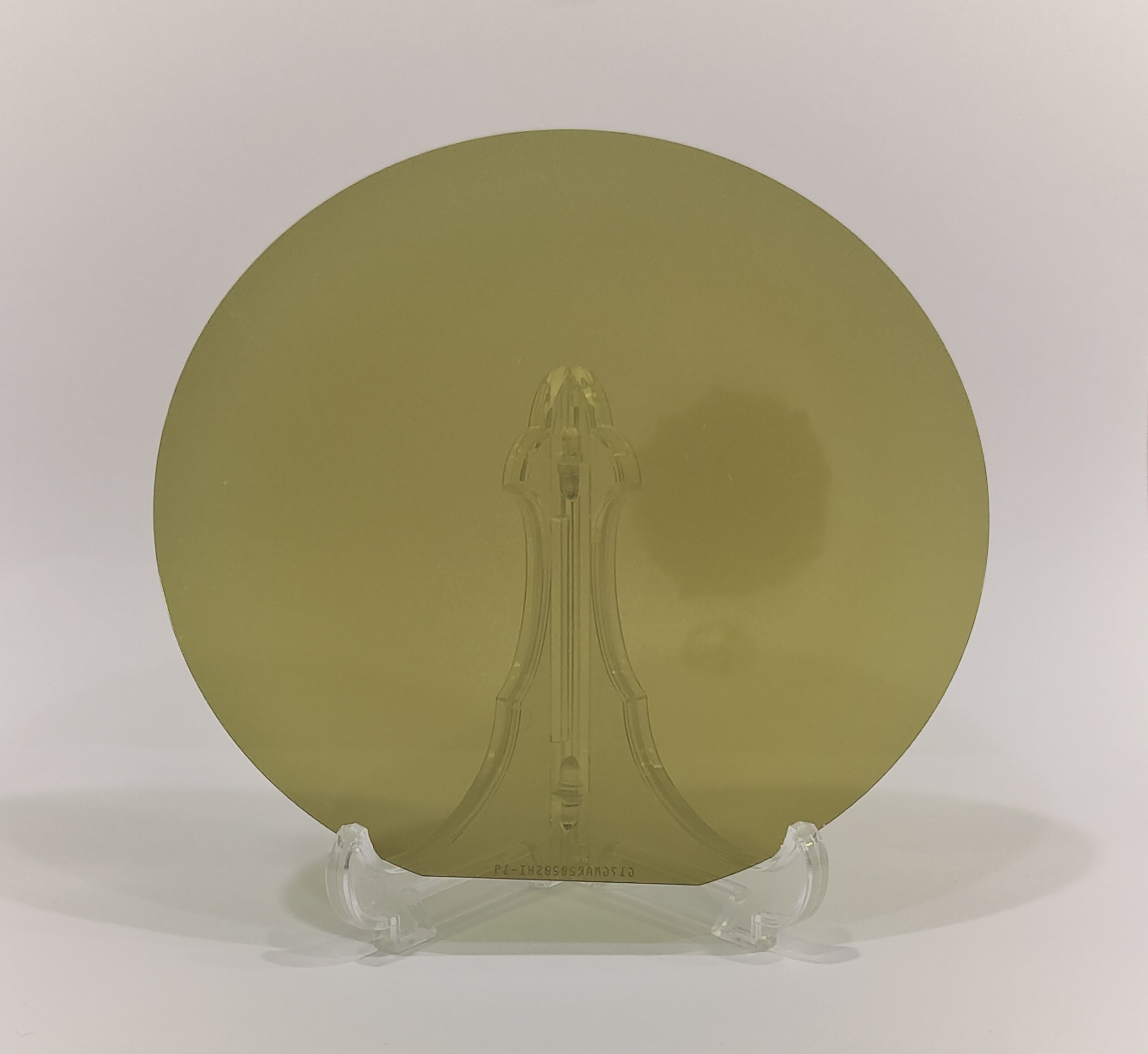


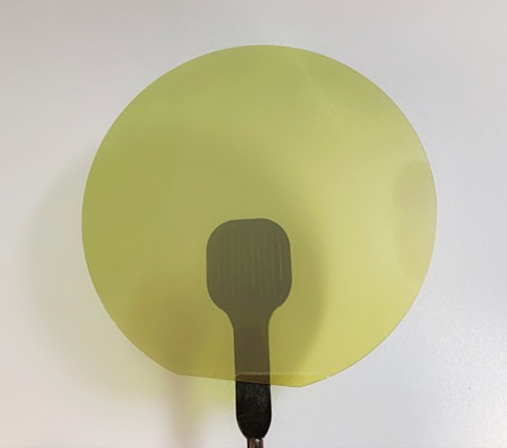
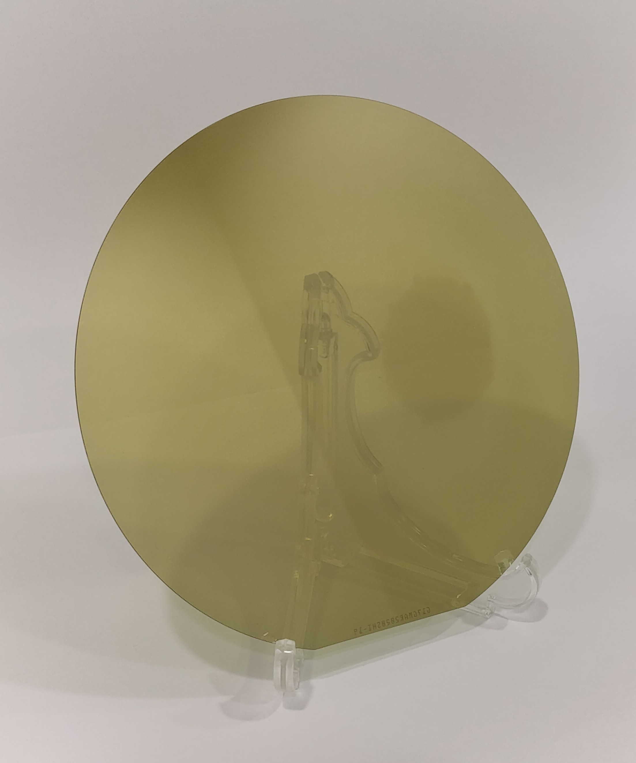
WaferLead was founded in Feb 2019, with the ambition of creating complete vertically integrated SiC ecosystem in Singapore to serve the global electronics market. SiC is the next generation material to improve the performance and efficiency of power electronics. Power devices made of SiC technology has ever-increasing applications in the fields of electric vehicles, charging units for electric vehicles, main and mini-grids, solid state transformers, locomotives, and PV and wind generators. Transition from Si devices to SiC devices directly and indirectly enables a huge energy saving, contributing to less greenhouse gas emissions to atmosphere. As the first leg of a long journey, WaferLead has started epi-SiC foundry business in early 2023. The unique feature of WaferLead epitaxial process is that it offers thicker SiC films up to 100 microns with minimum defects. That helps device manufactures to make MOSFET operating at higher voltages up to 10 kV.

Innovative yet affordable technologies enabling fast evolving power electronics industry.
Growing together with partners by providing empowering products. That will enable partners to lead the power electronics industry by constantly introducing innovative technological solutions to mass market resulting in elevated public safety, comfort, and living standards.
| Parameter | Value |
|---|---|
| Polytype | 4H, n-type |
| Dopant | Nitrogen |
| Resistivity | 15 - 25 mΩ・cm |
| Primary Surface | Si face |
| Orientation | (4± 0.5)° off-axis toward <11-20> |
| MPD | ≤ 1 cm-2 |
| Diameter | 150 ± 0.25 mm |
| Thickness | 350 ± 25 µm |
| Primary Flat Length | 47.5± 1.5 mm |
| Secondary Flat Length | no secondary flat |
| Primary Flat Position | <11-20> ± 3° |
| Surface Process | Si-face:CMP polished; epi-ready C-face: Optical polished |
| TTV | ≤10 µm |
| Warp | ≤40 µm |
| Bow | ±25 µm |
| LTV | ≤2 µm |

| Parameter | Value | |
|---|---|---|
| Buffer layer | Dopant | Nitrogen |
| Dopant concentration | 1x1018 cm-3 | |
| Epi thickness | 1 to 3 µm | |
| Drift layer | Thickness | 1 - 100 µm |
| Thickness uniformity | ≤3 % (EE=5mm, 30µm epi-layer) | |
| Thickness tolerance | ±5 % (for 30µm film) | |
| Dopant | Nitrogen | |
| Dopant concentration | 5x10¹⁵ -1x1019 cm-3 | |
| Dopant tolerance | ±15 % | |
| Dopant uniformity | ≤10 % (for 30µm film) | |
| Drift layer | Surface roughness (Ra) | < 0.5 nm |
| Metal contamination | <1 x10¹¹ atoms/cm2 | |
| Scratches | ≤ 1 x wafer diameter cumulative length | |
| TTV | ≤15 µm | |
| Warp | ≤50 µm | |
| Bow | ±30 µm | |
| LTV | ≤5 µm |